Potting electronics involves encapsulating electronic components or printed circuit boards (PCBs) within a solid mass of material. This process serves primarily to protect the electronics from various environmental factors, acting as a sturdy shell around delicate internal structures. The practice is widespread across numerous industries, from automotive and aerospace to telecommunications and consumer electronics.
Potting provides a robust shield for sensitive electronic assemblies. Its primary functions revolve around protection, though it also offers practical benefits in terms of assembly and security. Consider it as encasing a precious item in a durable, custom-fitted block.
Environmental Protection
One of the most critical roles of potting is safeguarding electronics from their surroundings. This includes a range of potential threats.
Moisture and Humidity
Water ingress is a significant cause of electronic failure. Even high humidity can lead to corrosion, short circuits, and degradation of insulating materials. Potting materials create a waterproof barrier, preventing moisture from reaching conductive parts. This is particularly vital in outdoor applications, marine environments, or medical devices where sterilization procedures might involve liquids.
Dust and Debris
Fine particles can accumulate on circuit boards, potentially shorting contacts or obstructing delicate moving parts (though less common in modern surface-mount technology). Potting encases the entire assembly, rendering it impervious to dust and other particulate contaminants. This is crucial in dusty industrial settings or environments with airborne metallic particles.
Chemical Exposure
Many industrial, automotive, and medical applications expose electronics to harsh chemicals, solvents, or oils. These substances can corrode traces, dissolve insulating layers, or degrade component packaging. Potting materials are often selected for their chemical resistance, forming an isolating layer that prevents corrosive substances from interacting with the electronics.
Vibration and Shock
Electronic components are susceptible to damage from mechanical stress. Constant vibrations can loosen connections or fatigue solder joints, while sudden impacts can cause components to break or detach from the PCB. The potting compound acts as a dampening agent, distributing mechanical forces across the entire encapsulated assembly rather than localizing them at specific components. This significantly improves the resilience of the device in demanding applications, such as automotive engine compartments or aerospace systems.
Temperature Extremes and Cycling
Rapid or extreme temperature changes can cause expansion and contraction of components and their connections, leading to stress fractures over time. Potting materials, especially those with matched coefficients of thermal expansion to the components, can mitigate these stresses by providing a thermally stable environment. They also help in heat dissipation for moderately heated components, acting as a thermal bridge to the external casing, though for high-power devices, specialized thermal management solutions are often combined with potting.
When it comes to potting electronics, understanding the various design considerations is crucial for ensuring optimal performance and durability. A related article that delves deeper into this topic is titled “Design Considerations for Overmolding and Insert Molding,” which provides valuable insights into the processes and factors that influence the effectiveness of potting materials. You can read more about it by following this link: Design Considerations for Overmolding and Insert Molding. This resource can help you make informed decisions when selecting materials and techniques for protecting electronic components.
Types of Potting Materials
The selection of a potting material is critical and depends on the specific application requirements. These materials are typically thermosetting polymers, meaning they undergo an irreversible chemical reaction to cure into a solid.
Epoxy Resins
Epoxies are widely used owing to their versatility and excellent properties. They are known for their strong adhesion, good chemical resistance, and high mechanical strength. However, they can be rigid after curing, which might be a disadvantage if thermal expansion mismatches are significant.
Advantages of Epoxies
Epoxy resins offer robust protection against impact, chemicals, and moisture. They often have good electrical insulation properties and can withstand higher temperatures compared to some other potting compounds. Their relatively long pot life (the time during which the mixed resin remains workable) allows for careful dispensing.
Disadvantages of Epoxies
A trade-off with epoxies is their rigidity. This can generate stress on delicate components during thermal cycling if the epoxy and component have different rates of expansion. Some epoxies can also be brittle, meaning they crack under impact rather than deforming. Reworking potted assemblies is typically very difficult or impossible with epoxies.
Polyurethane Resins
Polyurethanes are more flexible than epoxies, which makes them suitable for applications where thermal cycling or vibration damping is a primary concern. They can be formulated with a wide range of hardnesses.
Advantages of Polyurethanes
Their flexibility allows polyurethanes to absorb stress from thermal expansion mismatches, reducing strain on components. They also offer good adhesion and resistance to moisture. The ability to formulate them with varying degrees of hardness provides significant design flexibility.
Disadvantages of Polyurethanes
Some polyurethanes can be susceptible to hydrolysis, meaning they can degrade in the presence of water over long periods. They may also have lower chemical resistance or thermal stability compared to some epoxy formulations. Curing times can vary significantly, and some require specific humidity conditions for optimal curing.
Silicone-Based Compounds
Silicones are highly flexible and maintain their properties over a very wide temperature range, making them ideal for extreme environments.
Advantages of Silicones
Silicones excel in applications requiring high flexibility, excellent temperature stability (both high and low), and good dielectric properties. They are also resistant to UV radiation and provide good cushioning against shock and vibration. Their soft nature makes some degree of rework potentially feasible, though still challenging.
Disadvantages of Silicones
Generally, silicones have lower mechanical strength and adhesion compared to epoxies and polyurethanes. They can also be more expensive. Outgassing of certain compounds during cure or operation can be an issue in sensitive applications, such as optics or vacuum systems.
Other Materials
Other materials like acrylics and various thermoplastic elastomers (TPEs) also find niche applications in potting, often chosen for specific properties like UV resistance, transparency, or ease of processing.
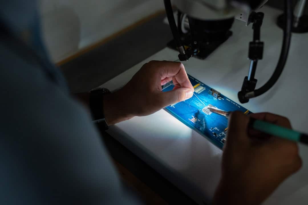
The Potting Process

The process of potting involves several critical steps that must be executed carefully to ensure the integrity and effectiveness of the encapsulation. This is not simply about pouring a liquid and letting it set; it’s a controlled manufacturing procedure.
Preparation of the Assembly
Before potting, the electronic assembly must be meticulously prepared. This often involves cleaning the PCB to remove any flux residues, oils, or other contaminants that could interfere with adhesion or cause electrical issues later. Components that require thermal dissipation, such as power transistors or voltage regulators, might need special attention.
Cleaning and Drying
Surfaces are typically cleaned with isopropyl alcohol or specialized solvents in ultrasonic baths, followed by thorough drying. Any residual moisture can lead to voids during potting or compromise the material’s properties. Consider this like preparing a canvas before painting; a clean surface ensures proper adhesion and a flawless finish.
Masking and Fixturing
Areas not intended for potting, such as connectors, switches, or LEDs, are masked off. The assembly is then placed in a potting fixture or mold that defines the shape and extent of the potting. This mold could be the device’s external enclosure itself or a temporary shell. This step ensures that the potting material goes only where it is intended and maintains the desired form.
Mixing and Degassing
Most potting compounds consist of two or more parts (resin and hardener) that must be thoroughly mixed in precise ratios. Air bubbles introduced during mixing or trapped within the compound can create voids, which act as weak points, compromising insulation and mechanical protection.
Automated Mixing Equipment
For consistent results and high-volume production, automated mixing and dispensing equipment is often employed. These systems ensure accurate ratios and thorough mixing, minimizing human error.
Vacuum Degassing
After mixing, the compound is often subjected to a vacuum to remove trapped air bubbles. Degassing creates a denser, more uniform encapsulate. Imagine air bubbles as tiny Achilles’ heels in the protective armor; degassing removes them to create an impermeable shield.
Dispensing and Curing
The mixed and degassed potting compound is then precisely dispensed into the prepared assembly and allowed to cure.
Dispensing Methods
Dispensing can be manual for small batches or automated for production lines. The compound is usually poured slowly to prevent further air entrapment, allowing it to flow and fill all voids around the components. Care must be taken to ensure complete coverage without overflowing masked areas.
Curing Conditions
Curing involves the chemical reaction that transforms the liquid resin into a solid. This process is time and temperature dependent. Some materials cure at room temperature, while others require heat (oven curing) to accelerate the reaction and achieve optimal properties. The curing schedule (temperature profile and duration) is specific to each potting compound and must be followed carefully. Incomplete curing can lead to a soft, sticky, or brittle encapsulate.
Design Considerations for Potting

Effective potting is not just about material selection and process execution; it also involves thoughtful design of the electronic assembly itself.
Component Selection and Layout
Components can react differently to potting materials and the curing process. Selecting components that are robust enough to withstand the thermal and mechanical stresses of potting is crucial.
Heat Generation
Components that generate significant heat (e.g., power ICs) need careful consideration. While potting can help with heat dissipation in some cases by increasing the thermal mass and surface area, too much heat can degrade the potting compound or lead to premature component failure. Heatsinks may need to be integrated into the design or ventilation provided around critical components.
Stress Sensitivity
Some components, such as delicate surface-mount devices (SMDs) or micro-electromechanical systems (MEMS), can be sensitive to the mechanical stresses induced by the shrinking of potting material during cure or by thermal expansion mismatches. Flexible potting compounds or design measures to relieve stress might be necessary.
Enclosure Design
The enclosure plays a significant role in the potting process, often acting as the mold itself. Its material, geometry, and features can greatly influence the success of potting.
Material Compatibility
The enclosure material must be compatible with the potting compound, meaning it should not react adversely with it and should provide good adhesion. Some plastics, for example, may require surface treatment to ensure proper bonding.
Potting Volume and Weight
The volume of potting compound directly impacts the weight of the final device. In weight-sensitive applications (e.g., aerospace, portable devices), this is a critical parameter. Designers might choose lighter potting materials or minimize the potted area where possible. The enclosure’s design must accommodate the required volume without excess.
Thermal Management
For applications where heat dissipation is critical, the enclosure and potting material must work together to conduct heat away from the electronics. This might involve metal enclosures functioning as heatsinks, or thermal pads and gaps to facilitate heat transfer from potted components to the enclosure.
When it comes to potting electronics, understanding the best practices can significantly enhance the durability and performance of your devices. A related article that delves deeper into this topic is available at Overmold Express, where you can find insights on materials and techniques that ensure optimal protection for electronic components. By exploring these resources, you can make informed decisions that will ultimately lead to more reliable and long-lasting electronic products.
Challenges and Limitations of Potting
| Metric | Description | Typical Values | Units |
|---|---|---|---|
| Potting Compound Dielectric Strength | Ability of the potting material to resist electrical breakdown | 15,000 – 25,000 | Volts per mm (V/mm) |
| Thermal Conductivity | Rate at which heat passes through the potting material | 0.2 – 1.5 | W/m·K |
| Shore Hardness | Measure of the hardness of the potting compound | 20 – 90 | Shore A or D |
| Cure Time | Time required for the potting compound to fully cure | 30 – 240 | Minutes |
| Operating Temperature Range | Temperature range in which the potted electronics can operate safely | -40 to 150 | °C |
| Volume Resistivity | Resistance to electrical conduction through the potting material | 10^12 – 10^15 | Ohm·cm |
| Coefficient of Thermal Expansion | Degree to which the potting material expands with temperature | 30 – 100 | 10^-6 /°C |
| Moisture Absorption | Amount of moisture absorbed by the potting compound over time | 0.1 – 1.0 | % weight gain |
While potting offers significant benefits, it also presents certain challenges and limitations that must be acknowledged.
Rework and Repair Difficulty
Perhaps the most significant limitation of potting is the difficulty, and often impossibility, of repairing or reworking a potted assembly. Once cured, the potting compound typically forms an inseparable bond with the components. This means that if a single component fails or an alteration is needed, the entire potted assembly often has to be scrapped, leading to increased waste and cost.
Destructive Removal
Removing potting material usually involves destructive methods like grinding, heating, or chemical dissolution, which invariably damage the underlying electronics. This characteristic makes potting a “one-way street” for most assemblies.
Thermal Management Issues
While potting can help dissipate heat in some scenarios, for high-power devices, it can act as a thermal insulator, trapping heat within the encapsulation. This can lead to overheating and premature failure of components. Careful thermal analysis and integration of heatsinks or thermal vias are often necessary.
Hot Spots
Even if overall heat dissipation is adequate, localized hot spots can still develop around individual high-power components within the pot, leading to localized degradation of the potting compound or component failure.
Cost and Process Complexity
The materials themselves can be expensive, and the potting process requires dedicated equipment, skilled operators, and controlled environments. This adds to the overall manufacturing cost and complexity, making it less suitable for low-cost, high-volume consumer electronics where ease of repair is also desired.
Material Handling and Storage
Many potting compounds have specific storage requirements (e.g., temperature, humidity, shelf life) and safe handling procedures due to their chemical nature. This further adds to the operational complexity.
Environmental Impact
The disposal of potted electronic waste presents environmental challenges. The combination of plastics, metals, and various chemicals in a solid, inseparable mass makes recycling difficult. Efforts are being made to develop more environmentally friendly potting compounds and more efficient recycling methods.
In conclusion, potting electronics is a robust and effective method for protecting devices from diverse environmental threats. Its application varies based on the specific needs of the electronic assembly, the operating environment, and the chosen potting material. While it introduces complexities in manufacturing and limits reparability, the enhanced reliability and longevity it imparts make it an indispensable technique in numerous critical applications where electronic integrity is paramount.
Give us a call to discuss your next project
FAQs
What is potting in electronics?
Potting in electronics refers to the process of encasing electronic components in a solid or gelatinous compound to protect them from moisture, dust, vibration, and other environmental factors.
What materials are commonly used for potting electronic components?
Common potting materials include epoxy resins, silicone compounds, polyurethane, and acrylics. Each material offers different levels of protection, flexibility, and thermal conductivity.
Why is potting important for electronic devices?
Potting enhances the durability and reliability of electronic devices by providing insulation, preventing corrosion, reducing mechanical stress, and improving resistance to environmental hazards.
Can potted electronics be repaired or reworked?
Potting generally makes repair or rework difficult because the components are encapsulated in a solid material. In many cases, the potting compound must be removed carefully, which can risk damaging the components.
Are there any disadvantages to potting electronics?
Disadvantages include increased weight and size of the device, difficulty in repairing or recycling components, and potential thermal management challenges if the potting material does not dissipate heat effectively.
